- 您现在的位置:买卖IC网 > Sheet目录471 > MAX1472EVKIT-433# (Maxim Integrated)EVAL KIT MAX1472
300MHz-to-450MHz Low-Power,
Crystal-Based ASK Transmitter
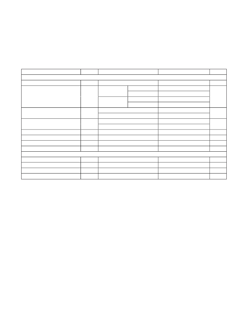
ELECTRICAL CHARACTERISTICS (continued)
( Typical Application Circuit , output power is referenced to 50 ? , V DD = 2.1V to 3.6V, V ENABLE = V DD , T A = -40 ° C to +125 ° C, unless
otherwise noted. Typical values are at V DD = 2.7V, T A = +25 ° C, unless otherwise noted.) (Note 1)
PARAMETER
SYMBOL
CONDITIONS
MIN
TYP
MAX
UNITS
PHASE-LOCKED LOOP PERFORMANCE
VCO Gain
330
MHz/V
Phase Noise
Maximum Carrier Harmonics
Reference Spur
Loop Bandwidth
f RF = 315MHz
f RF = 433MHz
f RF = 315MHz
f RF = 433MHz
f RF = 315MHz
f RF = 433MHz
f OFFSET =100kHz
f OFFSET = 1MHz
f OFFSET =100kHz
f OFFSET = 1MHz
-84
-91
-82
-89
-50
-50
-75
-81
1.6
dBc/Hz
dBc
dBc
MHz
Crystal Frequency
Oscillator Input Capacitance
Frequency Pushing by V DD
f XTAL
From each XTAL pin to GND
f RF / 32
6.2
3
MHz
pF
ppm/V
DIGITAL INPUTS
Data Input High
Data Input Low
Maximum Input Current
Pulldown Current
V IH
V IL
V DD - 0.25
2
25
0.25
V
V
nA
μA
Note 1:
Note 2:
Note 3:
Note 4:
Note 5:
Note 6:
Note 7:
Note 8:
Note 9:
100% tested at T A = +25°C. Guaranteed by design and characterization over temperature.
50% duty cycle at 10kHz data.
Guaranteed by design and characterization, not production tested.
Generally limited by PC board layout.
Output power can be adjusted with external resistor.
Guaranteed by design and characterization at f RF = 315MHz.
V ENABLE < V IL to V ENABLE > V IH . f OFFSET is defined as the frequency deviation from the desired carrier frequency.
V ENABLE > V IH , V DATA > V IH , Efficiency = P OUT /(V DD x I DD ).
V ENABLE > V IH , DATA toggled from V IL to V IH , 10kHz, 50% duty cycle, Efficiency = P OUT /(V DD x I DD ).
3
发布紧急采购,3分钟左右您将得到回复。
相关PDF资料
MAX1473EVKIT-433
EVAL KIT MAX1473
MAX1479EVKIT-315
EVAL KIT FOR MAX1479 315MHZ
MAX19700EVKIT
EVAL KIT FOR MAX19700
MAX19985AETX+T
IC MIXER DOWNCONV 36-TQFN-EP
MAX19993ETX+
IC MIXER DOWNCONV 36TQFN
MAX19994AEVKIT#
KIT EVAL FOR MAX19994A MIXER
MAX19995ETX+T
IC DOWNCONVERTER 2CH 36TQFN
MAX19995EVKIT#
EVALUATION KIT FOR MAX19995
相关代理商/技术参数
MAX1473ETJ
制造商:Maxim Integrated Products 功能描述:315MHZ/433MHZ ASK SUPERHETERODYNE RECEIVER WI - Rail/Tube
MAX1473ETJ+
功能描述:射频接收器 315MHz/434MHz Superheterodyne Rcvr RoHS:否 制造商:Skyworks Solutions, Inc. 类型:GPS Receiver 封装 / 箱体:QFN-24 工作频率:4.092 MHz 工作电源电压:3.3 V 封装:Reel
MAX1473ETJ+T
功能描述:射频接收器 315MHz/434MHz Superheterodyne Rcvr RoHS:否 制造商:Skyworks Solutions, Inc. 类型:GPS Receiver 封装 / 箱体:QFN-24 工作频率:4.092 MHz 工作电源电压:3.3 V 封装:Reel
MAX1473ETJ-T
制造商:Maxim Integrated Products 功能描述:315MHZ/433MHZ ASK SUPERHETERODYNE RECEIVER WI - Tape and Reel
MAX1473EUI
功能描述:射频接收器 RoHS:否 制造商:Skyworks Solutions, Inc. 类型:GPS Receiver 封装 / 箱体:QFN-24 工作频率:4.092 MHz 工作电源电压:3.3 V 封装:Reel
MAX1473EUI/V+
功能描述:射频接收器 315MHz/434MHz Superheterodyne Rcvr RoHS:否 制造商:Skyworks Solutions, Inc. 类型:GPS Receiver 封装 / 箱体:QFN-24 工作频率:4.092 MHz 工作电源电压:3.3 V 封装:Reel
MAX1473EUI/V+T
功能描述:射频接收器 315MHz/434MHz Superheterodyne Rcvr RoHS:否 制造商:Skyworks Solutions, Inc. 类型:GPS Receiver 封装 / 箱体:QFN-24 工作频率:4.092 MHz 工作电源电压:3.3 V 封装:Reel
MAX1473EUI+
功能描述:射频接收器 315MHz/434MHz Superheterodyne Rcvr RoHS:否 制造商:Skyworks Solutions, Inc. 类型:GPS Receiver 封装 / 箱体:QFN-24 工作频率:4.092 MHz 工作电源电压:3.3 V 封装:Reel
